“The advantages of ultrasonic bonding include low thermal input, short processing times, high mechanical strength and the possibility of joining different materials. This makes the process particularly suitable for advanced modules such as power components, RF components, MEMS and LED housings,”
”Despite the numerous advantages, there are also challenges such as procurement costs, process optimization and material compatibility. However, ongoing research and development efforts in the market and on our part are aimed at solving these challenges and thereby paving the way for a broader introduction and integration of ultrasonic DIE bonding into automated manufacturing processes.”
Daniel Schultze, Managing Director of Tresky GmbH
Schultze would therefore like to provide a comprehensive overview of the ultrasonic DIE bonding process, its mechanisms and the possibility of its application in modern semiconductor manufacturing, in order to familiarize the professional community with the advantages of the process. In particular, the demand for smaller, faster, and more powerful electronic devices has led to innovations in semiconductor packaging technology. Ultrasonic bonding has become the method of choice for processing heat-sensitive chips due to its ability to create reliable bonds with minimal thermal stress.
Ultrasonic bonding can therefore be an alternative to thermocompression bonding in flip chip bonding. In flip chip bonding, a row of gold bumps on the bottom side of an IC are connected to gold-plated pads on a substrate.
“Pure thermocompression bonding usually requires interface temperatures in the range of ≥ 280 °C. This temperature can damage packaging materials, laminates and some sensitive microchips.”
Daniel Schultze
Ultrasonic bonding is an alternative to flip chip bonding because the interface temperature and bonding force here are usually between 100 and 160 °C respectively 20 and 50 g/bump and thus cause less material stress.
“The high-frequency ultrasonic vibrations generate local heating at the interface between the chip and the substrate, which leads to the formation of a stable bond.”
Daniel Schultze
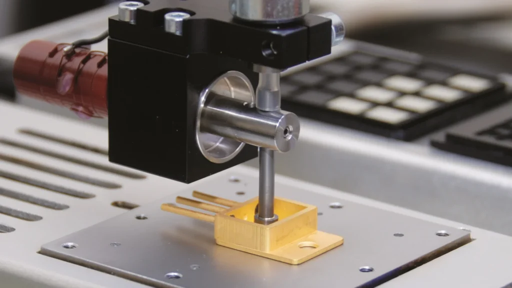
Various individual steps are necessary to ensure that the process is carried out reliably. This includes cleaning the surfaces of the DIE and the substrate and preparing them to ensure an optimal bond. The chip is held by a DIE collet, which must be suitable for ultrasonic bonding. After the DIE is aligned on the substrate by the Tresky pattern recognition system, the DIE is precisely positioned and exposed to controlled pressure. The ultrasonic energy that is introduced causes the surfaces to vibrate. These vibrations break up the surface oxides and impurities, enabling contact at the atomic level. The ultrasonic parameters, i.e. power, time and delay, are adjustable in the Tresky DIE Bonder machine software. The combination of pressure and ultrasonic energy creates a solid-state connection, whereby the materials are plastically formed and diffuse. This allows reproducible, stable bonds to be created between the DIE and the substrate.
