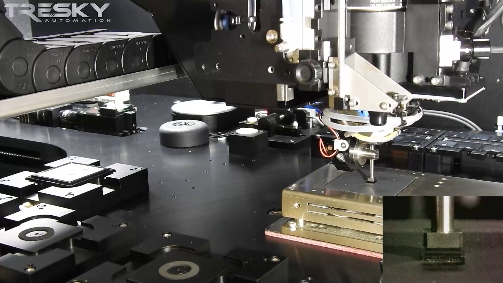
High-precision connection technology for temperature-sensitive components
Ultrasonic bonding is a bonding process for creating an electrically conductive and mechanically cohesive connection between a chip and a substrate. This method uses high-frequency ultrasonic vibrations to create a reliable connection between semiconductor chips and substrates. The ultrasonic energy is applied when the chip is placed by the bonding head, which significantly reduces the thermal load compared to conventional methods.
The advantages of ultrasonic bonding include low thermal input, short processing times, high mechanical strength and the possibility of bonding different materials. This makes the process particularly suitable for advanced modules such as power components, HF-components, MEMS and LED housings. In particular, the demand for smaller, faster and more powerful electronic devices has led to innovations in semiconductor packaging. This is where ultrasonic bonding has become the preferred method for processing heat-sensitive chips, since it can achieve reliable connections with minimal thermal stress.
White Paper
Ultrasonic Bonding in semiconductor industry – The fast and clean process

The efficiency of the ultrasonic DIE bonder is determined by several variable parameters, such as bonding force, ultrasonic power, frequency and bonding time. These factors play a crucial role in ensuring the quality and reliability of the connections produced.
Ultrasonic bonding offers an alternative to thermo-compression bonding in flip chip bonding. In flip chip bonding, a row of gold bumps on the underside of an IC are connected to gold-plated pads on a substrate. Pure thermo-compression bonding normally requires interface temperatures in the range of ≥280°C. However, this temperature range can damage packaging materials, laminates and some sensitive microchips. With interface temperatures of typically 100 and 160°C and bond forces of 20 and 50 g/bump, this process reduces material stress. The high-frequency ultrasonic vibrations ensure targeted local heating at the interface between the chip and the substrate, resulting in a stable connection.
Added Values
Cycle Time Optimization
Ultrasonic bonding allows shorter bonding times to be implemented due to the elimination of preheating time
High Power Density
Ultrasonic bonding enables the production of high-performance components with high power density.
Low Thermal Load
The process generates a lower thermal load compared to conventional bonding methods. This can reduce material stress on semiconductor components.
Reliability
Connections made by ultrasonic bonding are reliable and have low failure rates. This is critical to the quality and durability of electronic components.
Versatility
Ultrasonic bonding can be used with a wide range of materials and chip types, increasing its versatility in various applications.
No Joining Materials
For example, in radio frequency (RF) applications, adhesive or solder joints are often ruled out because they radically degrade signal quality. Ultrasonic bonding creates a direct connection without a connecting layer.
Miniaturization
Ultrasonic bonding enables the miniaturization of electronic components and thus contributes to the development of compact and powerful electronic devices.
Variable Parameters for Ultrasonic Bonding are
- Bond force (pressure)
- Ultrasonic power (energy)
- Frequency (vibration)
- Bonding time