Home / Technologies
Technologies
DIE Attach/ DIE Bonding Overview
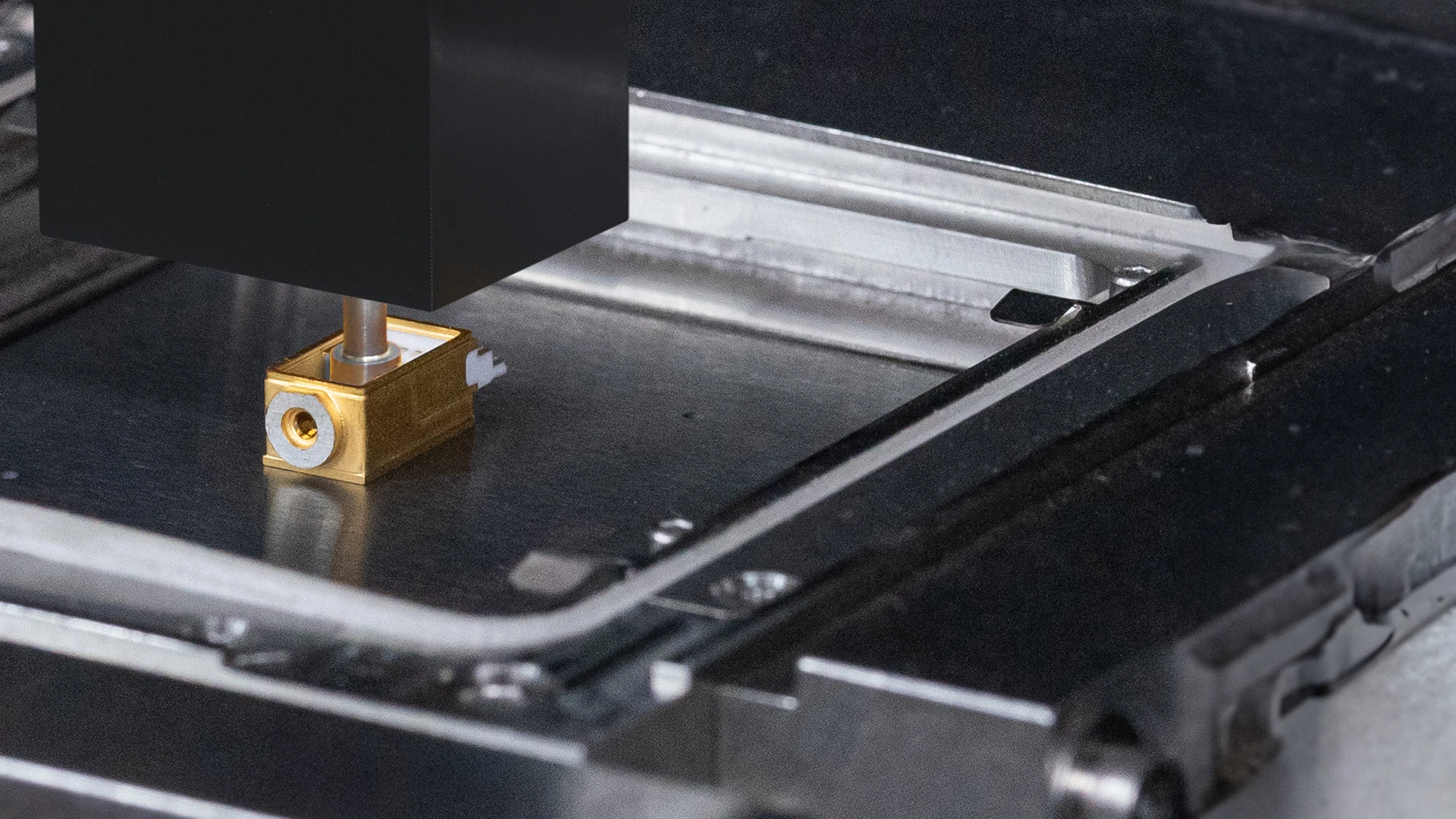
DIE Attach or DIE Bonding are the generic terms for the process of permanently connecting a semiconductor chip to a substrate, package, wafer or other component.
Epoxy/Adhesive DIE Bonding
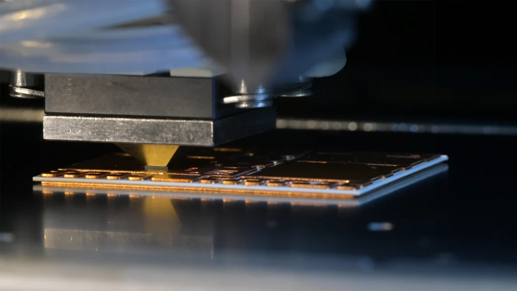
One of the most common methods for creating a bond between chip and substrate, is the epoxy DIE bonding process. The first step involves applying the conductive or non-conductive adhesive, typically described as the epoxy adhesive or “epoxy” for short. This step involves various methods (needle dosing, stamping, jetting, etc.). Next step involves placing the DIE into the epoxy by the machines vacuum pick and place bond head. The adhesive is then cured using heat within a supplier defined temperature and cure time.
Variable parameters
- Adhesive quantity
- Dispensing pattern
- Dispenser air pressure
- Dispenser dwell time
Advantages
- Low contact pressure on the chip
- Low to no thermal load on the chip
UV DIE Bonding
UV DIE Bonding is a special bonding technology in which liquid adhesive is cured using ultraviolet (UV) light. Unlike epoxy, which requires different times and temperatures to cure depending on the type of adhesive, UV adhesive, on the other hand, remains in its liquid state until it is exposed to high-energy UV radiation.
The advantages of this technology are that the UV adhesive does not readily cure until the UV light source is proactively applied. UV epoxies have a longer work life and offer a much shorter cure time. Cure time with UV light exposure is usually only a few seconds.
This technology is often used for inline processes as well as for temperature-sensitive components.
Variable parameters
- Adhesive quantity
- Dispensing pattern
- Dispenser air pressure
- Dispenser dwell time
Advantages
- Low contact pressure on the chip
- Low to zero thermal stress
- on the chip
Freely definable curing time - Fast curing
Ultrasonic Bonding (US Bonding)
Ultrasonic Bonding is a bonding process for producing an electrically conductive and mechanical bond between the chip and a substrate. In the cold friction welding process, pressure and ultrasonic vibration (friction) are used to create an electrical conductive connection.
Since the process can be used at room temperature, unlike Thermosonic Bonding, no additional substrate heating is required. Temperature-sensitive components or components that are difficult to heat can be processed by Ultrasonic Bonding.
Variable parameters
- Bond force (pressure)
- Ultrasonic power (energy)
- Frequency (vibration)
- Ultrasonic application time
Advantages
- Reduction of bonding time
- No additional heat required
Thermocompression Bonding (TC Bonding)
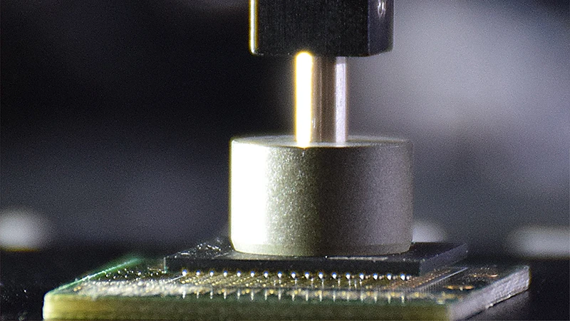
Thermocompression Bonding is an electrically conductive, mechanically solid and flux-free bonding process. In most cases, TC Bonding involves placing a Flip Chip with bumps on a substrate with pads. By applying force and temperature over a defined time, an electrically conductive contact is created.
TC bonding is particularly suitable for RF & optoelectronic devices. Such as chip to chip and chip to wafer applications. Typical alloy compounds to be mentioned here are Au-Au and Au-Si.
Variable parameters
- Bonding force (pressure)
- Work Holder Temperature
- Collet Temperature
- Ultrasonic application time
Advantages
- High bond strength
- Electrically conductive bond connection
Metallic Sinter Bonding
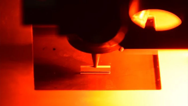
During the sintering process, the chip is bonded to the substrate by silver paste, not only electrically but also thermally. This is done with the aid of heat (above 220°C) and a pressure of at least 50 bar up to 300 bar. The silver particles are bonded together by diffusion processes. The advantage over normal soldering processes is the very high thermomechanical stability, which is required above all in power electronics.
Dispensing of Tacking Agent for High Power Module assembly
A tacking agent can be used to hold and fix preforms, dies or chips in place after placement. This prevents the placed component from moving during the subsequent transport or during further process steps or from being able to get into a crooked position. The advantage of a tack agent is that it can be
easily applied to the printed sinter paste by means of dispensing or jetting through the DIE Bonder. This contributes in particular to improving reliability.
in sintering and vacuum soldering.
DIE Stacking
DIE Stacking is an assembly process in which several chips are stacked on top of each other on a substrate. This vertical integration allows a compact arrangement of different circuits with different dimensions on a very small area, which not only saves space but also achieves higher performance in the component due to shorter signal paths between the circuits.
The interconnection technologies are adapted to the specific requirements of the application.
Variable parameters
- Number of stacked DIE
Advantages
- Space savings, high chip density
- Shorter signal paths
- Reduction of run times and noise
- Possible combinations with Flip Chip technology increase above mentioned advantages
Flip Chip Bonding
Flip Chip Bonding is also known as C4 technology (Controlled Collapse Chip Connection). It is an assembly and vertical interconnection technology (AVT) process for contacting bare DIE semiconductor chips by means of balls – so-called “bumps”.
In Flip-Chip assembly, the chip is mounted directly, without any further connecting wires. The active and bumped contacting side is facing downwards – towards the substrate/circuit carrier. Hence the name flip chip. This results in particularly small package dimensions and short conductor lengths. In very complex circuits, this technology is often the only sensible connection option, because in some cases several thousand contacts have to be realized. This means that the entire surface of the DIE can be used to make connections.
Such dense connections are not possible with wire bonding. High density wire bonding risks wire loop shorting as a result of wire sway between the first and second bond. Furthermore, in wire bonding, the connections are made one after the other. With flip-chip bonding, all contacts are connected at the same time. This saves time.
Variable parameters
- Bonding force (pressure)
- Work Holder Temperature
- Collet Temperature
- Ultrasonic application time
Advantages
- High package density with limited space requirements
- Shorter signal paths / higher frequencies
DIE Sorting
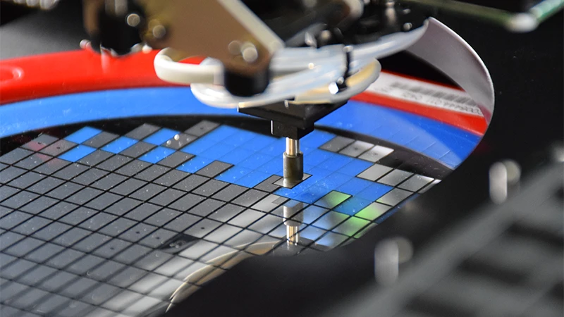
Die Sorting is the re-sorting or re-organization of semiconductor chips from one component presentation (source) into another component presentation (destination). Often chips are re-sorted from a wafer (source) into a waffle pack (destination). However, there is also the re-sorting into belts, gel packs or other component presentations media.
Variable parameters
- Storage locations
Advantages
- Increasing the number of DIE for multichip applications
- Structured component presentation
Eutectic Bonding
Eutectic bonding connects chip and substrate to form a eutectic system, by means of an intermediate layer. This bonding process exploits the specific properties of the individual materials and alloy mixtures during “bonding”. The frequently used gold/tin (AuSn 80/20) alloy has its melting point at 280 °C, while a gold/silicon (AuSi) alloy finds its melting point at 363 °C.
The advantage of the alloy combinations is that their melting point is significantly lower than that of the individual materials. When heat is applied, a “liquid phase” forms above the eutectic temperature, which diffuses causing bonding in the atomic range. Another significant advantage of eutectic bonding is that the chip and the substrate are electrically and mechanically connected in a single process step.
Variable parameters
- Work Holder Temperature
- Collet Temperature
- Ramp Heating and Ramp Cooling
Advantages
- Hermetically sealed connections
- Lower temperatures possible compared to thermocompression
